
Sandia National Laboratories selects LayTec’s EpiX® for advanced optical wafer characterization
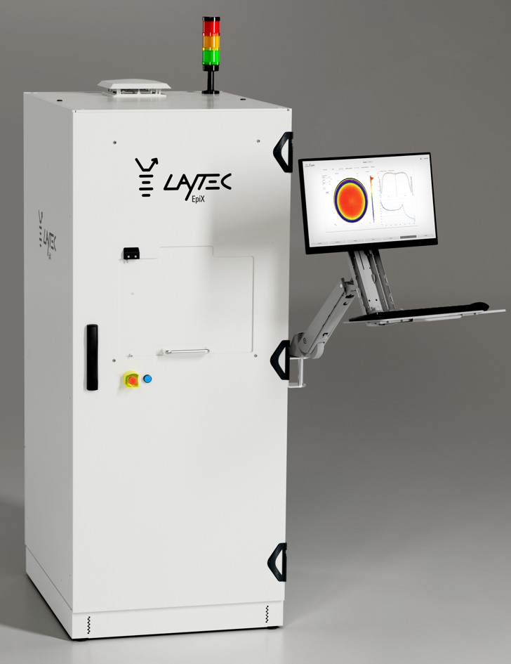
Berlin, Germany – July 1, 2026 – Sandia National Laboratories has purchased a customizedmanual-loading version of LayTec’s EpiX® mapping station, co mbining white light reflectance (WLR) and photoluminescence (PL) metrology for non-contact optical wafer mapping.
The system comes in a UV-VIS configuration optimized for AlGaN power, RF, and optoelectronic applications, as well as novel materials, supporting Sandia’s advanced semiconductor research by providing spatially resolved insight into key wafer properties. EpiX® uniquely enables 2D mapping of parameters such as layer thickness, composition-related optical signatures and luminescence characteristics for high electronic-mobility transistors and other device structures, helping researchers evaluate uniformity across complex semiconductor wafers.
“We are pleased that Sandia has selected LayTec’s EpiX® platform for its research environment,” says Volker Blank, CEO of LayTec. “The customized configuration reflects exactly what EpiX® was designed for: flexible, high-quality optical wafer characterization for demanding compound semiconductor R&D.”

For more information, please contact: Volker Blank, CEO and Director Marketing & Sales at LayTec, Email: info@laytec.de, T: +49 (0)30 89 00 55 0.
Download the press release as a PDF here: