A new 280 nm perspective on Ga₂O₃ growth: LayTec’s customized EpiTT 4W is now supporting IKZ’s research into next-generation power electronics
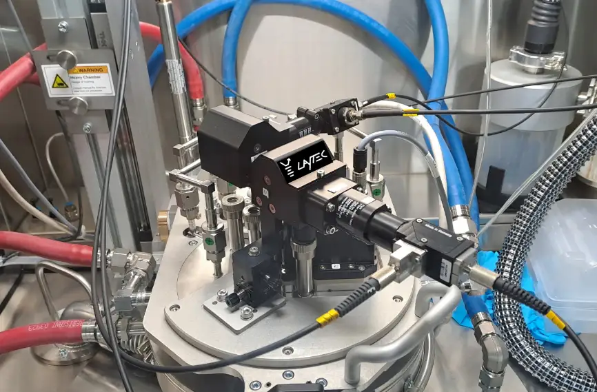
Berlin, Germany, July 23 , 2026 – LayTec AG, a leading provider of in-situ metrology solutions for thin-film processes, is pleased to announce the successful installation of a newly enhanced EpiTT 4W system with additional ultraviolet reflectometry at 280 nm at the Leibniz-Institut für Kristallzüchtung (IKZ). This upgraded system, namely the 4000th measurement system provided by LayTec, will play a key role in cutting edge research on gallium oxide (Ga₂O₃) epitaxy, a material increasingly recognized for its potential in next generation power electronics.
The new 280 nm channel expands the established EpiTT measurement capabilities, allowing researchers to gain deeper insight into early stage growth dynamics and surface processes of wide bandgap materials like gallium oxide.
With its unique combination of emissivity corrected pyrometry and reflectivity monitoring, the EpiTT has already demonstrated its value in analyzing growth rates, doping levels, and surface morphology during epitaxy. The additional UV wavelength now promises even greater sensitivity for
more accurate observation of surface roughness/morphology changes
analysis of very thin films
interface formation and early nucleation stages
particularly for materials like gallium oxide, which exhibit strong absorption in the deep UV range, but also for other materials grown by epitaxial processes.
Gallium oxide, a material with strong future potential
Gallium oxide has attracted significant attention as one of the most promising ultra wide-bandgap semiconductors. Its exceptionally high breakdown field and compatibility with cost effective substrate production make it an attractive candidate for next generation high power, high efficiency electronic devices. These characteristics could enable smaller, more efficient power converters and open new paths for energy saving technologies across multiple industries.
Strengthening research collaboration
With the project G.O.A.L. (“Gallium Oxide Application Laboratory for Power Electronics”), led by Dr. Andreas Popp, the Leibniz-Institut für Kristallzüchtung (IKZ) is expanding its research and development infrastructure in the field of innovative semiconductor materials. The aim of the project is to establish an integrated technological platform for the semiconductor material gallium oxide (Ga₂O₃) for applications in power electronics. The project is co-financed by the European Regional Development Fund (Europäischer Fonds für regionale Entwicklung, EFRE). The acquisition of the MOVPE system from AIXTRON, including the in-situ monitoring system from LayTec, represents the core investment of the project. Without this expansion of technical infrastructure, made possible by the project, the implementation of the project objectives would not be feasible.
The new EpiTT system will support the work of the research group Gallium Oxide Epitaxy in the section Application Science at the IKZ. The group is very enthusiastic about the expanded measurement capabilities now available and expect the system to deliver valuable new insights into gallium oxide epitaxy and the fundamental mechanisms that govern its growth. Also, the new IKZ Spin-off NextGO Epi GmbH which aims to commercialize Ga₂O₃ Epi-Wafer will benefit from the new LayTec tool. LayTec is proud to support the IKZ team and NextGO Epi with state of the art metrology in this rapidly advancing research field,” said the company. “Together, we aim to accelerate progress toward the next generation of semiconductor materials.”
About IKZ:
The Leibniz-Institut für Kristallzüchtung (IKZ) in Berlin-Adlershof belongs to the Leibniz Association and, together with six other Leibniz Institutes, is organised within the Forschungsverbund Berlin e.V. The IKZ is an international state-of-the-art competence center for science & technology as well as service & transfer for innovations in and by crystalline materials. The R&D spectrum thereby ranges from basic over applied research activities up to pre-industrial research tasks. Crystalline materials are key technology enabling components to provide electronic and photonic solutions to today´s and future challenges in society such as artificial intelligence (communication, mobility etc.), energy (renewable energies, power conversion etc.) and health (medical diagnosis, modern surgical instruments etc.).
About LayTec:
LayTec, part of the Nynomic group, is a Berlin-based company which designs and manufactures integrated in-situ and in-line optical metrology solutions for process control in semiconductor and photovoltaic production. LayTec provides metrology systems for non-destructive monitoring for critical film properties, including thickness, color, band gap, sheet resistance, composition and surface roughness. These systems cover a broad spectrum of deposition and film formation techniques, supporting both academic research and high-volume industrial production. With over 4000 systems installed worldwide, LayTec supports both research and mass production environments and offers a global service network to ensure reliable performance and customer success.
For more information, please contact: Volker Blank, CEO and Director Marketing & Sales at LayTec, Email: info@laytec.de, T: +49 (0)30 89 00 55 0.
Download the press release as a PDF here: